


Exploring Advanced Techniques in Chip Bonding
- Nov 18, 2025
- 4 min read
In the world of semiconductor manufacturing, the process of connecting microchips to their substrates is critical. This connection ensures the functionality and reliability of electronic devices. Over the years, advancements in technology have led to the development of sophisticated techniques that improve the efficiency, precision, and durability of chip connections. This article delves into some of the most advanced chip bonding methods, offering insights into their mechanisms, benefits, and practical applications.
Understanding Advanced Chip Bonding Methods
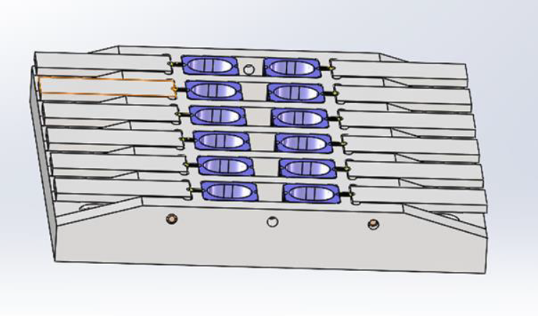
Advanced chip bonding methods have revolutionized the way microchips are assembled and integrated into electronic systems. These techniques go beyond traditional wire bonding and flip-chip bonding, incorporating innovative materials and processes to meet the demands of modern electronics.
Some of the prominent advanced methods include:
Thermocompression Bonding: This method uses heat and pressure to create a strong metallic bond between the chip and substrate. It is highly reliable and suitable for fine-pitch applications.
Thermosonic Bonding: Combining ultrasonic energy with heat and pressure, this technique enhances bond strength and reduces the risk of damage to delicate components.
Anisotropic Conductive Film (ACF) Bonding: ACF bonding uses a conductive adhesive film that allows electrical connection only in the vertical direction, preventing short circuits and enabling high-density interconnections.
Laser-Assisted Bonding: Utilizing focused laser beams, this method precisely heats bonding areas, allowing for localized bonding without affecting surrounding components.
Each of these methods offers unique advantages depending on the application, materials involved, and desired performance characteristics.

How Easily Does a Bonding Chip?
The ease of bonding a chip depends on several factors including the bonding method, chip size, substrate material, and environmental conditions. For example, thermocompression bonding requires precise control of temperature and pressure to avoid damaging the chip or substrate. On the other hand, ACF bonding is relatively easier to perform as it involves applying a conductive adhesive film and curing it under controlled heat.
Key considerations for ease of bonding include:
Surface Preparation: Clean and smooth surfaces promote better adhesion and electrical contact.
Alignment Accuracy: Precise alignment tools are essential to ensure that bonding pads on the chip and substrate match perfectly.
Process Parameters: Optimizing temperature, pressure, and time settings is crucial for achieving strong and reliable bonds.
Material Compatibility: The bonding materials must be compatible with both the chip and substrate to prevent issues like delamination or corrosion.
By carefully managing these factors, manufacturers can streamline the bonding process, reduce defects, and improve overall yield.
Innovations Driving Chip Bonding Technology
Recent innovations have pushed the boundaries of what is possible in chip bonding. These advancements address challenges such as miniaturization, thermal management, and mechanical stress.
Nano-Scale Bonding: Techniques that enable bonding at the nanometer scale allow for ultra-fine pitch connections, essential for next-generation microelectronics.
Flexible Substrate Bonding: With the rise of wearable and flexible electronics, bonding chips to bendable substrates has become a focus area. New adhesives and bonding methods accommodate mechanical flexibility without compromising electrical performance.
3D Integration: Stacking chips vertically using through-silicon vias (TSVs) and advanced bonding methods increases device density and performance.
Environmentally Friendly Processes: Green bonding techniques reduce the use of hazardous materials and energy consumption, aligning with sustainability goals.
These innovations not only enhance device capabilities but also open new possibilities for applications in fields like IoT, automotive electronics, and medical devices.
Practical Tips for Implementing Advanced Bonding Techniques
For engineers and technicians looking to adopt advanced chip bonding methods, here are some actionable recommendations:
Invest in Precision Equipment: High-quality bonding machines with accurate temperature and pressure controls are essential.
Train Personnel Thoroughly: Skilled operators can significantly reduce bonding defects and improve throughput.
Conduct Rigorous Testing: Perform electrical, mechanical, and thermal tests to validate bond integrity.
Optimize Process Parameters: Use design of experiments (DOE) to find the best combination of bonding conditions.
Maintain Cleanroom Standards: Contaminants can severely impact bond quality, so strict cleanliness is a must.
By following these guidelines, manufacturers can maximize the benefits of advanced bonding methods and ensure product reliability.
Future Trends in Chip Bonding
The future of chip bonding is poised for exciting developments driven by emerging technologies and market demands. Some trends to watch include:
Integration with AI and Machine Learning: Automated bonding systems powered by AI can optimize processes in real-time, reducing errors and increasing efficiency.
Hybrid Bonding Techniques: Combining multiple bonding methods to leverage their strengths and overcome limitations.
Enhanced Thermal Management: New materials and bonding structures that improve heat dissipation for high-power devices.
Miniaturization and High-Density Packaging: Continued push towards smaller, more powerful devices will require innovative bonding solutions.
Staying informed about these trends will help industry professionals prepare for the next generation of semiconductor manufacturing challenges.
For more detailed insights and updates on chip bonding, exploring specialized resources and technical blogs is highly recommended.
By embracing advanced chip bonding methods, the electronics industry can achieve higher performance, greater reliability, and innovative product designs that meet the evolving needs of technology users worldwide.


Comments