top of page


Optical Module Guide: Demystifying Optical Modules and Their Uses
what is an optical module
1 day ago5 min read


The Impact of cw-wdm technology solutions
CWDM technology solutions are particularly valuable in metropolitan area networks (MANs) and data centers where space and cost constraints are significant.
5 days ago4 min read


50G PON Advancements: The Next Frontier
50G PON represents a significant leap from previous generations like 10G and 25G PON. It offers a fivefold increase in data transmission speeds, enabling service providers to deliver ultra-fast internet to homes and businesses.
5 days ago4 min read


Optical Module Guide: Demystifying Optical Modules and Their Uses
Optical modules are essential components in modern communication networks, enabling high-speed data transmission over fiber optic cables. As the demand for faster and more reliable internet and data services grows, understanding these devices becomes increasingly important. This guide will explore the fundamentals of optical modules, their types, applications, and how they differ from similar technologies. Optical Module Guide: Understanding the Basics Optical modules are com
Jan 274 min read


Effective 50G PON Solutions with EML-SOA Benefits
The demand for faster and more reliable internet connections continues to grow exponentially. To meet this demand, Passive Optical Networks (PON) have evolved significantly, with 50G PON emerging as a leading technology for high-speed broadband access. One of the key enablers of this advancement is the integration of Electro-absorption Modulated Laser with Semiconductor Optical Amplifier (EML-SOA) technology. This blog post explores the effective 50G PON solutions powered by
Jan 134 min read


Optimizing 140gbd Optical Performance with IC-TROSA Technology
Optical performance at 140 gigabaud (GBd) represents a leap in data transmission speed and efficiency.
Dec 30, 20254 min read


Understanding Optical Modules: A Comprehensive Guide
Optical Module Basics: Understanding the Core Concepts Optical modules are compact devices that convert electrical signals into optical signals and vice versa. They are used in fiber optic communication systems to transmit data over long distances with minimal loss and interference. These modules typically consist of a laser or LED transmitter, a photodiode receiver, and supporting electronics. The primary function of an optical module is to enable communication between netwo
Dec 23, 20254 min read


Understanding CW-WDM Technology Explained
In the world of optical communications, CW-WDM technology plays a crucial role in enhancing data transmission efficiency. This technology is especially important for modern data centers and telecommunication networks that demand high bandwidth and reliable connectivity. Understanding how CW-WDM works and its applications can help businesses and network engineers optimize their infrastructure for better performance. CW-WDM Technology Explained: Basics and Benefits CW-WDM stan
Dec 16, 20253 min read


Understanding Semiconductor Bonding Techniques
Understanding Semiconductor Chip Bonding Techniques
Nov 24, 20254 min read


Exploring Advanced Techniques in Chip Bonding
Understanding Advanced Chip Bonding Methods,How Easily Does a Bonding Chip?
Nov 18, 20254 min read


How Advanced Chip Bonding Enhances Semiconductor Reliability
How Advanced Chip Bonding Enhances Semiconductor Reliability
Nov 11, 20254 min read


Mastering the Art of Semiconductor Chip Bonding
Semiconductor chip assembly is a critical process in the electronics industry, enabling the creation of compact, high-performance devices. This intricate procedure involves connecting tiny semiconductor chips to substrates or packages, ensuring electrical and mechanical integrity. Mastering this art requires understanding various bonding techniques, materials, and challenges that impact the final product's reliability and efficiency.
Nov 4, 20254 min read


How Coatings Enhance Optical Performance and Durability
How Coatings Enhance Optical Performance and Durability
Oct 21, 20254 min read


The Future of Packaging for High-Tech Electronics
Hermetically sealed HTCC ceramic packages for RF, microwave, and sensor modules.
Available in 50Ω / 100Ω impedance with durable multilayer structure.
Precision ceramic bases and lids for hybrid microelectronic packaging.
Material options: Aluminum Nitride (AlN) or Alumina (Al₂O₃), with gold or Ni/Au plating
Supports custom pin layouts, leadframes, and glass-sealed designs
Ideal for RF modules, power devices, and high-reliability hermetic circuits
Oct 15, 20254 min read


Why Sapphire is Ideal for Optical Applications
Sapphire optics have become a cornerstone in many high-performance optical systems. Their unique properties make them an excellent choice for applications requiring durability, clarity, and precision.
Oct 10, 20253 min read


Understanding IC Packaging: Common Failure Modes and Solutions
IC packaging failures and controls. Key modes: wire-bond lift-off, solder-ball voiding/insufficiency, die cracking and interfacial fracture, substrate delamination, and reflow warpage. Mitigations include precision stencil printing, optimized nitrogen/vacuum reflow and ramp rates, improved pastes with lifecycle humidity control, low-CTE substrates/RDL/TSV reinforcement, and inline 3D metrology, X-ray, C-SAM, FEM and AI analytics, achieving void <3%, warpage ≤50 μm, and >99.9%
Oct 7, 20253 min read


Understanding the Basics of Semiconductor Chip Assembly
Embracing the Future of Semiconductor Assembly
Oct 6, 20254 min read


Exploring the Benefits of Anti-Reflective Coatings
How to Choose the Right Anti-Reflective Coating
Sep 29, 20254 min read


The Evolution of Packaging in Electronics Manufacturing
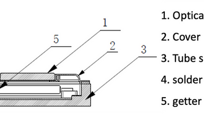
Infrared Package Structure
Aug 8, 20254 min read


How Tailored Solutions Meet Unique Industrial Needs
In today's fast-paced industrial environment, businesses are continually seeking ways to optimize their processes and improve efficiency....
Jul 4, 20253 min read
bottom of page
